Xian Hadia
PhD Candidate & Electrical Engineer

Georgia Institute of Technology
School of Computational Science and Engineering
Atlanta, GA 30332
I am a Ph.D. candidate in Computational Science and Engineering at Georgia Tech, advised by Prof. Raphaël Pestourie. My research lies at the intersection of computational electromagnetics, inverse design, and photonic engineering, with an emphasis on developing high-performance computational frameworks for solving complex electromagnetic design problems.
I develop high-fidelity, computationally efficient electromagnetic solvers to enable scalable inverse design of photonic devices under practical fabrication constraints. My work combines adjoint-based optimization, data-driven surrogate modeling, and high-performance computing to make the optimization of high-dimensional electromagnetic systems computationally tractable.
A central goal of my research is bridging the gap between numerical simulation and physical realization. Beyond computational methods, I have hands-on experience in photonic device fabrication, optical metrology, experimental characterization, and automation. I have taken photonic designs through the complete workflow, from numerical simulation and optimization to fabrication and experimental validation.
See my recent publications on Google Scholar.
Research Keywords: Photonics, Computational Electromagnetics, Inverse Design, Adjoint Optimization, Scientific Computing
Here’s some of what I do:
Much of my work involves solving partial differential equations (PDEs) across complex geometries, materials, and boundary conditions—most notably, Maxwell’s equations, which govern electromagnetic phenomena.
Although electromagnetism is well understood theoretically, accurately and efficiently solving Maxwell’s equations for complex, high-dimensional photonic systems remains a significant computational challenge. This shifts modern photonic engineering from a problem of physics to numerical methods and scientific computing.
My research focuses on developing efficient electromagnetic solvers and physics-based surrogate models that balance computational cost with physical fidelity, enabling scalable simulation, optimization, and inverse design.

Beyond simulating electromagnetic phenomena, a central goal of my research is to design photonic devices with prescribed optical responses.
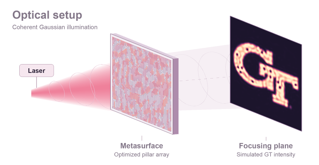
Consider a metasurface composed of subwavelength nanostructures that manipulate light. Even a device just 1 mm in diameter, with individually tunable structures on a 400 nm period, can contain nearly five million design parameters. How do you even begin to search through this enormous design space?
Inverse design addresses this challenge by formulating the desired engineering function as a mathematical optimization problem. Rather than manually adjusting device geometries, we iteratively optimize their design parameters to maximize a chosen performance objective.
One particularly powerful approach is adjoint optimization, which enables the gradient of a scalar objective with respect to millions of design parameters to be computed using just two electromagnetic solves: one forward and one adjoint, under appropriate assumptions.
Combined with high-performance electromagnetic solvers, this makes the optimization of otherwise computationally prohibitive photonic devices tractable.
The interactive demonstration below illustrates iterative metasurface design for optical wavefront shaping.

latest posts
| Aug 05, 2026 | Computational Electromagnetics: Finite Difference vs. Finite Element Method |
|---|---|
| Jan 30, 2026 | Electromagnetics: Propagation |
| Jan 27, 2026 | Electromagnetics: Sources |